- 您现在的位置:买卖IC网 > Sheet目录494 > NVD6415ANLT4G (ON Semiconductor)MOSFET N-CH 100V 23A DPAK-4
�� �
�
�NTD6415ANL,� NVD6415ANL�
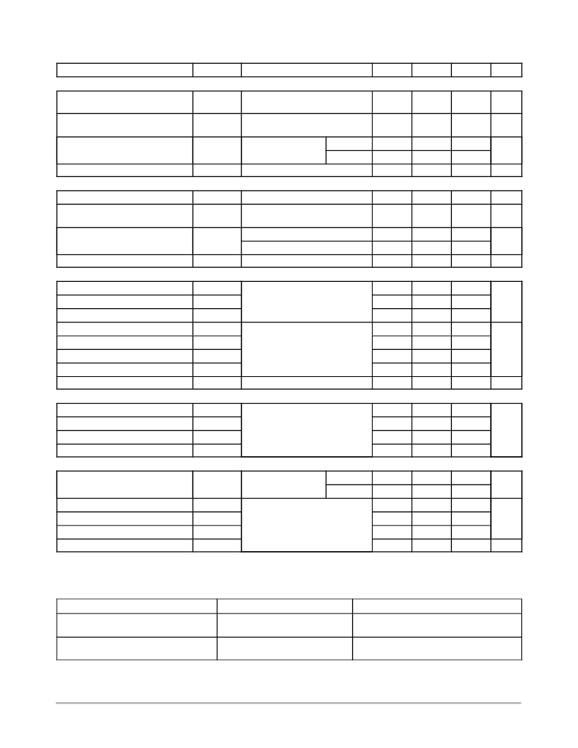
�ELECTRICAL CHARACTERISTIC� S� (T� J� =� 25� °� C� unless� otherwise� noted)�
�Parameter�
�Symbol�
�Test� Condition�
�Min�
�Typ�
�Max�
�Unit�
�OFF� CHARACTERISTICS�
�Drain� ?� to� ?� Source� Breakdown� Voltage�
�Drain� ?� to� ?� Source� Breakdown� Voltage�
�Temperature� Coefficient�
�V� (BR)DSS�
�V� (BR)DSS� /T� J�
�V� GS� =� 0� V,� I� D� =� 250� m� A�
�V� GS� =� 0� V,� I� D� =� 250� m� A,� T� J� =� ?� 40� °� C�
�100�
�92�
�115�
�V�
�mV/� °� C�
�Zero� Gate� Voltage� Drain� Current�
�I� DSS�
�V� GS� =� 0� V,�
�V� DS� =� 100� V�
�T� J� =� 25� °� C�
�T� J� =� 125� °� C�
�1.0�
�100�
�m� A�
�Gate� ?� to� ?� Source� Leakage� Current�
�I� GSS�
�V� DS� =� 0� V,� V� GS� =� "� 20� V�
�"� 100�
�nA�
�ON� CHARACTERISTICS� (Note� 2)�
�Gate� Threshold� Voltage�
�Negative� Threshold� Temperature�
�Coefficient�
�V� GS(TH)�
�V� GS(TH)� /T� J�
�V� GS� =� V� DS� ,� I� D� =� 250� m� A�
�1.0�
�4.8�
�2.0�
�V�
�mV/� °� C�
�Drain� ?� to� ?� Source� On� ?� Resistance�
�R� DS(on)�
�V� GS� =� 4.5� V,� I� D� =� 10� A�
�44�
�56�
�m� W�
�V� GS� =� 10� V,� I� D� =� 10� A�
�43�
�52�
�Forward� Transconductance�
�g� FS�
�V� DS� =� 5.0� V,� I� D� =� 10� A�
�24�
�S�
�CHARGES,� CAPACITANCES� AND� GATE� RESISTANCE�
�Input� Capacitance�
�C� ISS�
�1024�
�pF�
�Output� Capacitance�
�Reverse� Transfer� Capacitance�
�C� OSS�
�C� RSS�
�V� GS� =� 0� V,� f� =� 1.0� MHz,� V� DS� =� 25� V�
�156�
�70�
�Total� Gate� Charge�
�Q� G(TOT)�
�20�
�nC�
�Threshold� Gate� Charge�
�Gate� ?� to� ?� Source� Charge�
�Gate� ?� to� ?� Drain� Charge�
�Q� G(TH)�
�Q� GS�
�Q� GD�
�V� GS� =� 4.5� V,� V� DS� =� 80� V,� I� D� =� 23� A�
�1.1�
�3.1�
�14�
�Total� Gate� Charge�
�Q� G(TOT)�
�V� GS� =� 10� V,� V� DS� =� 80� V,� I� D� =� 23� A�
�35�
�nC�
�SWITCHING CHARACTERISTICS� (Not� e� 3)�
�Turn� ?� On� Delay� Time�
�t� d(on)�
�11�
�ns�
�Rise� Time�
�Turn� ?� Off� Delay� Time�
�Fall� Time�
�t� r�
�t� d(off)�
�t� f�
�V� GS� =� 4.5� V,� V� DD� =� 80� V,�
�I� D� =� 23� A,� R� G� =� 6.1� W�
�91�
�40�
�71�
�DRAIN� ?� SOURCE� DIODE� CHARACTERISTICS�
�Forward� Diode� Voltage�
�V� SD�
�V� GS� =� 0� V,� I� S� =� 23� A�
�T� J� =� 25� °� C�
�T� J� =� 125� °� C�
�0.87�
�0.74�
�1.2�
�V�
�Reverse� Recovery� Time�
�t� RR�
�64�
�ns�
�Charge� Time�
�Discharge� Time�
�T� a�
�T� b�
�V� GS� =� 0� V,� dI� S� /dt� =� 100� A/� m� s,�
�I� S� =� 23� A�
�40�
�24�
�Reverse� Recovery� Charge�
�Q� RR�
�152�
�nC�
�2.� Pulse� Test:� Pulse� Width� ≤� 300� m� s,� Duty� Cycle� ≤� 2%.�
�3.� Switching� characteristics� are� independent� of� operating� junction� temperatures.�
�ORDERING� INFORMATION�
�NTD6415ANLT4G�
�NVD6415ANLT4G�
�Device�
�Package�
�DPAK�
�(Pb� ?� Free)�
�DPAK�
�(Pb� ?� Free)�
�Shipping� ?�
�2500� /� Tape� &� Reel�
�2500� /� Tape� &� Reel�
�?For� information� on� tape� and� reel� specifications,� including� part� orientation� and� tape� sizes,� please� refer� to� our� Tape� and� Reel� Packaging�
�Specification� Brochure,� BRD8011/D.�
�http://onsemi.com�
�2�
�发布紧急采购,3分钟左右您将得到回复。
相关PDF资料
NVF2955PT1G
MOSFET P CH 60V 1.7A SOT223
NVF5P03T3G
MOSFET P-CH 30V 3.7A SOT-223
NVMFD5877NLT1G
MOSFET N-CH 60V 17A 8SOIC
NVMFS4841NT1G
MOSFET N-CH 30V 89A SO-8FL
NVMFS5844NLT1G
MOSFET N-CH 60V 11.2S SO-8FL
NVR1P02T1G
MOSFET N-CH 20V 1A SOT-23-3
NVTFS4823NTAG
MSOFET N-CH 30V 30A 8WDFN
NVTFS4824NTAG
MOSFET N-CH 30V 18.2A 8WDFN
相关代理商/技术参数
NVD6415ANT4G
功能描述:MOSFET
RoHS:否 制造商:STMicroelectronics 晶体管极性:N-Channel 汲极/源极击穿电压:650 V 闸/源击穿电压:25 V 漏极连续电流:130 A 电阻汲极/源极 RDS(导通):0.014 Ohms 配置:Single 最大工作温度: 安装风格:Through Hole 封装 / 箱体:Max247 封装:Tube
NVD6416ANLT4G
功能描述:MOSFET
RoHS:否 制造商:STMicroelectronics 晶体管极性:N-Channel 汲极/源极击穿电压:650 V 闸/源击穿电压:25 V 漏极连续电流:130 A 电阻汲极/源极 RDS(导通):0.014 Ohms 配置:Single 最大工作温度: 安装风格:Through Hole 封装 / 箱体:Max247 封装:Tube
NVD6416ANT4G
功能描述:MOSFET
RoHS:否 制造商:STMicroelectronics 晶体管极性:N-Channel 汲极/源极击穿电压:650 V 闸/源击穿电压:25 V 漏极连续电流:130 A 电阻汲极/源极 RDS(导通):0.014 Ohms 配置:Single 最大工作温度: 安装风格:Through Hole 封装 / 箱体:Max247 封装:Tube
NVD6820NL
制造商:ONSEMI 制造商全称:ON Semiconductor 功能描述:Power MOSFET 90 V, 17 m, 50 A, Single N.Channel
NVD6820NLT4G
功能描述:MOSFET NFET DPAK 90V 50A 17MOHM RoHS:否 制造商:STMicroelectronics 晶体管极性:N-Channel 汲极/源极击穿电压:650 V 闸/源击穿电压:25 V 漏极连续电流:130 A 电阻汲极/源极 RDS(导通):0.014 Ohms 配置:Single 最大工作温度: 安装风格:Through Hole 封装 / 箱体:Max247 封装:Tube
NVD6824NL
制造商:ONSEMI 制造商全称:ON Semiconductor 功能描述:Power MOSFET 100 V, 20 m, 41 A, Single N.Channel
NVD6824NLT4G
功能描述:MOSFET NFET DPAK 100V 40A 24MOHM RoHS:否 制造商:STMicroelectronics 晶体管极性:N-Channel 汲极/源极击穿电压:650 V 闸/源击穿电压:25 V 漏极连续电流:130 A 电阻汲极/源极 RDS(导通):0.014 Ohms 配置:Single 最大工作温度: 安装风格:Through Hole 封装 / 箱体:Max247 封装:Tube
NVD6828NL
制造商:ONSEMI 制造商全称:ON Semiconductor 功能描述:Power MOSFET 90 V, 20 m, 41 A, Single N.Channel